4 Bits Multiplier Design in Electric VLSI with VHDL Built Layout

4 Bits Multiplier is a combinational logic circuit used to multiply binary units in digital systems. Digital circuits are the base of computer systems. Still, those small circuit modules like multipliers, adders, and LUT, etc. are the substructures that create complex digital circuits. 4 Bits Multiplier is the one we obtain the multiplication of 2×2 Bits ( 01 x 10 = 0010 ). The design of these subcircuits and performance comparisons in regards to size, power, and speed will be covered in this article.
Add2 – Half Adder Module
Assume that A and B are 2 bits of 2 positive numbers and R is 4 bits output. Then the following equations will be occurred to calculate multiplication ;
- R0=B0.A0
- R1 , C1 = add2(B0.A1 , B1.A0)
- R2, C2 = add2(C1 , B1.A1)
- R3=C2
As it can be seen from the equation, the addition of 2 Bits is done by using a combinational circuit called Half- Adder (add2) at the digital logic level. Therefore, half adder has to be designed first to create a multiplier. Accordingly as a result of this addition, sum and carry values will be stored at the output.
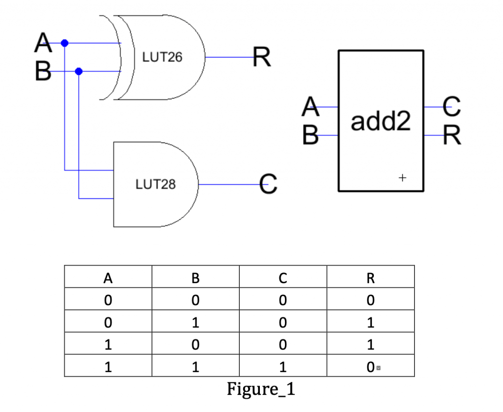
Basically, the half adder can be designed as Figure_1. LUTs(Lookup Table) represent the logic operations like XOR , OR , AND. Relatively, LUT table can be found at the end of the article. (LUT26(XOR) and LUT28(AND)). The sum is stored in the R variable and carry is in C. This was the basic logic circuit that will be needed during the design of the 2×2 multiplier.
Multiplier with Half Adders
Hence half adder (add2) is ready, a 2×2 Multiplier can be created as follows based on the derived equations for R0 , R1 , R2 , R3 bits ;
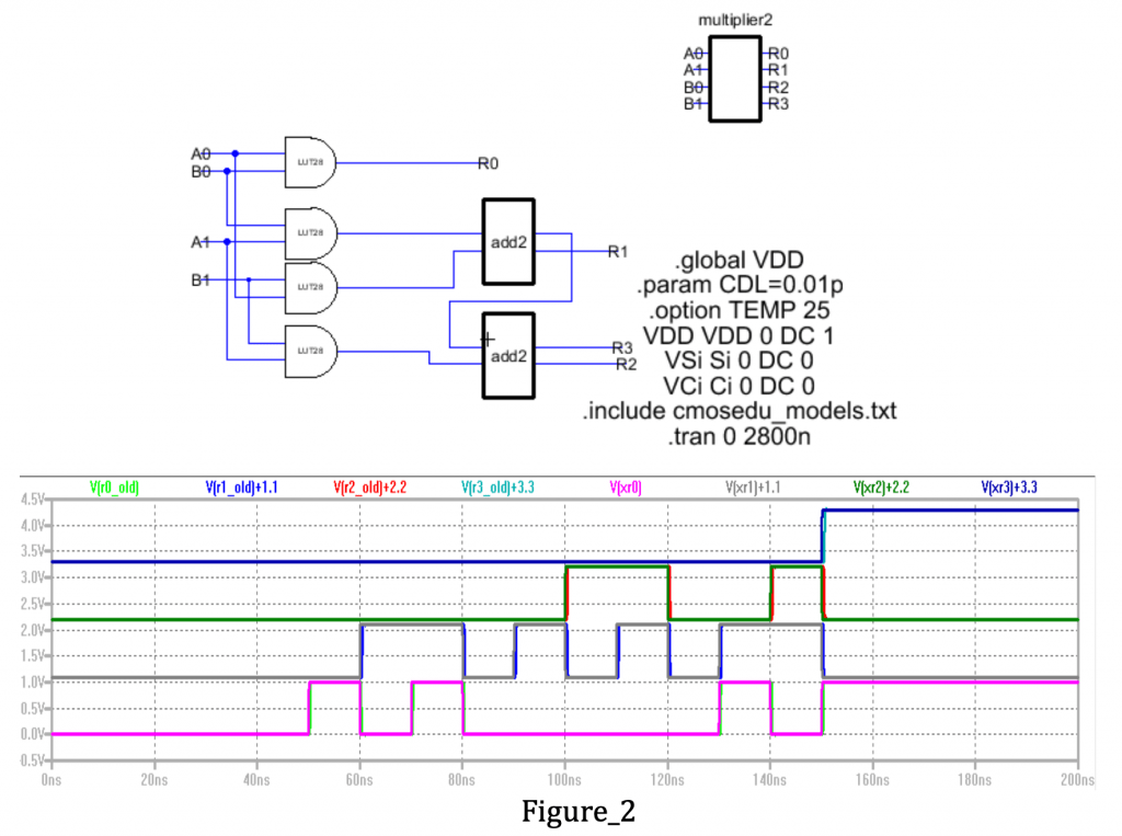
Simulation results are as shown in Figure__2 concerning Spice waveform(1). Delay calculations will be shared in further sections.
Since the functionality is confirmed with Spice, the next step will be creating a transistor layout with VLSI. There are two possible ways to do it; either from the logic circuit at Figure_2 or with the VHDL equivalent script as given below.
——————– Cell multiplier2{sch} ——————–
entity multiplier2 is port(A0, A1, B0, B1: in BIT; R0, R1, R2, R3: out BIT);
end multiplier2;
architecture multiplier2_BODY of multiplier2 is
component LUT28 port(I0, I1: in BIT; O: out BIT); end component;
component add2 port(A, B: in BIT; C, R: out BIT); end component;
signal net_13, net_15, net_4, net_9: BIT; begin
LUT28_0: LUT28 port map(B0, A1, net_13); LUT28_1: LUT28 port map(B1, A0, net_15); LUT28_2: LUT28 port map(B1, A1, net_9);
LUT28_3: LUT28 port map(A0, B0, R0);
add2_0: add2 port map(net_13, net_15, net_4, R1); add2_1: add2 port map(net_4, net_9, R3, R2);
end multiplier2_BODY;
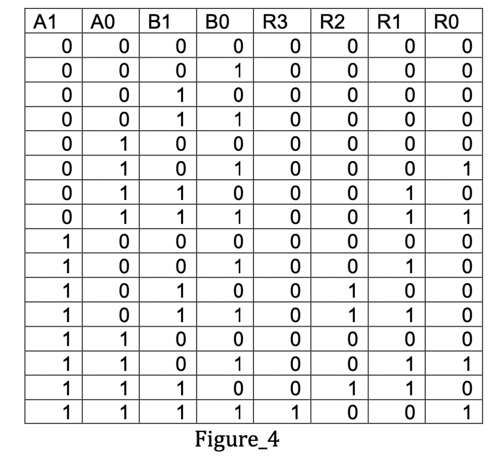
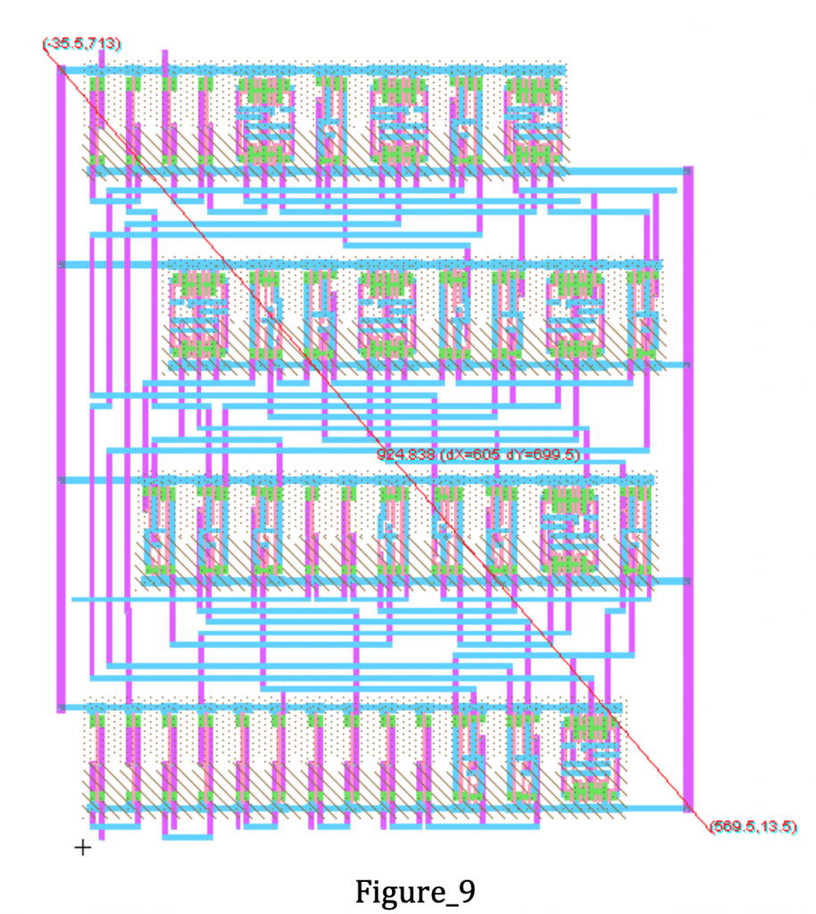
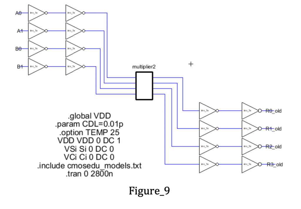
Each logic circuit has to be tested with load and driver LUTs to do reliable propagation delay measurements. For this logic, circuit inverters are used as load and driver. For this purpose, the layout of the design is created by load and driver added schematic (Figure_9) version, and relevant VHDL code is also presented. The area of the design was also measured as 405(lambda) * 443(lambda). The truth table of the 4 bits multiplier as shown in Figure_4 and confirms the functionality.
Addx – Full Adder Module
It was mentioned at the beginning of the study as well, there should be at least two multipliers to make a performance comparison. The second multiplier will be created with the full adders.
Full adder is another type of adder that has 3 inputs. 3rd input enables to carry in – transfer from the previous operation in addition to the 2 inputs. Basically, described by the OR gate connection of carry outputs of two half adders. The importance of this full adder circuit can be more visible if the 3×3 multiplier design process is considered. There are two and three AND operations with carry output that should be added together. That needs six half adders for R2 output. Quantity of used gates matters for more complex circuits.
The following equations are derived to structure the 4 bits multiplier` logic circuit ;
- R0 = A0.B0
- R1,C1 = A1.B0 +A0.B1
- R2,C2=C1+(A2.B0+A1.B1+A0.B2)
- R3,C3 = C2 + (A2.B1 + A1.B2)
- R4,C4 = C3 + A2.B2 •R5 =C4
It can be easily understood from the equations which gates will be needed for this operation.
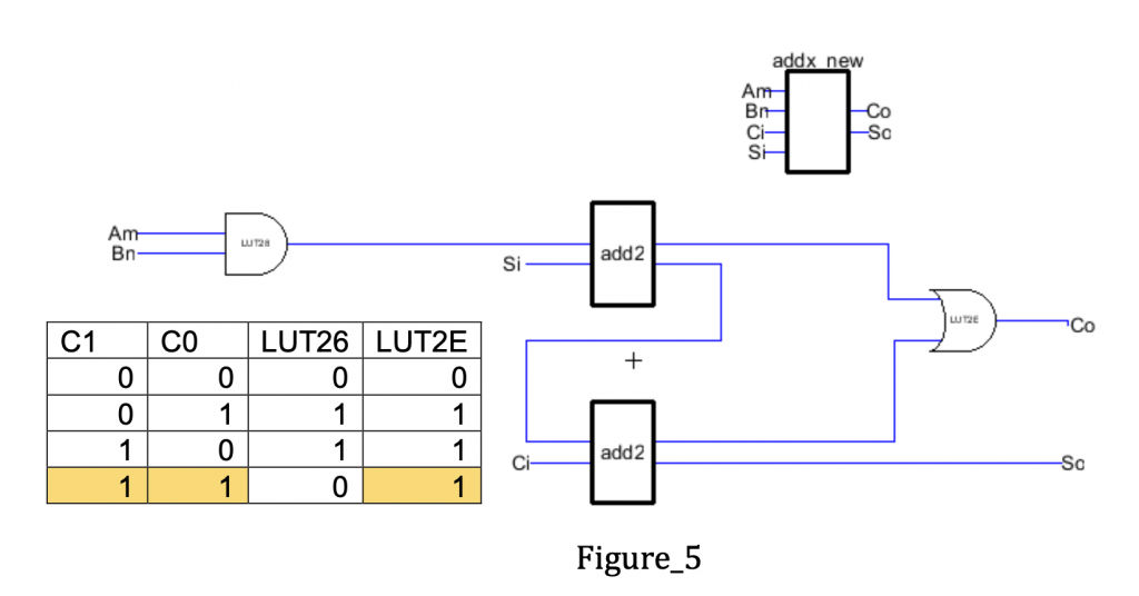
A simple logic design is created based on the discussed rules above. ( 2 Half adder and carry outputs are connected with OR gate ).LUT2E or LUT26 can be used for this design since the yellow marked situation never going to happen. Due to the reason that LUT2E has fewer transistors, it will cause less delay.
The next step is to create a multiplier that uses addx_new full adder for adding operation.
2×2 Multiplier with Full Adder
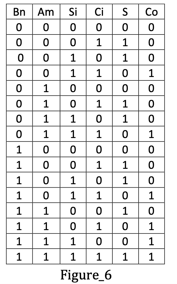
The given truth table indicates the addx last Sum and Carry outputs. S= Bn.Am + Si + Ci is the Boolean function of the Sum.
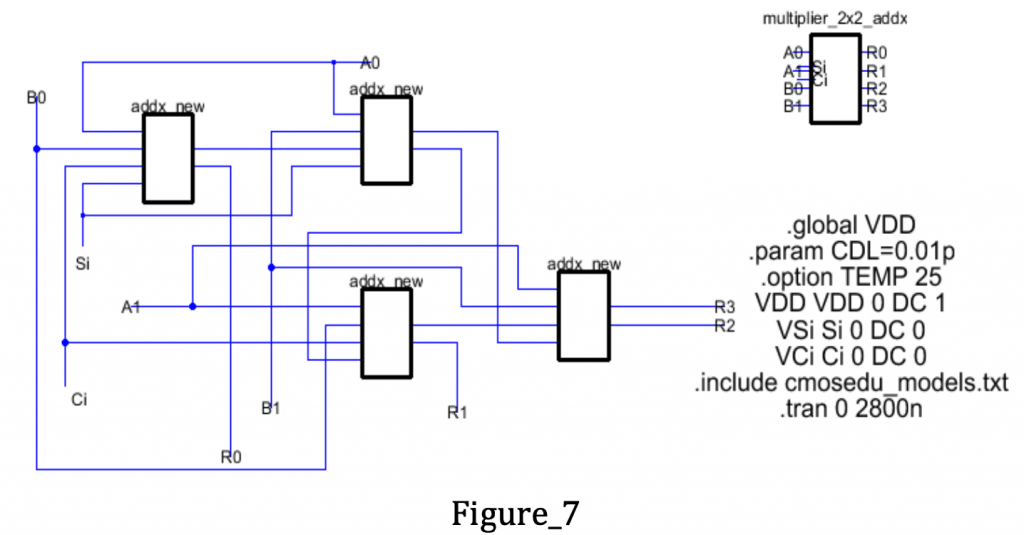
The structured logic circuit is based on carry propagation between adders as it was explained in add2. Si and Ci inputs should be defined as 0 initially since there is no sum and carry value available. Shortly, with the interconnection of 4 full adders, the multiplier can be designed in the same manner. Accordingly, the truth table at Figure_4 is valid also for this logic circuit too.
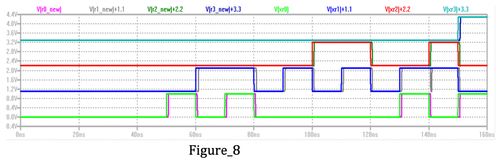
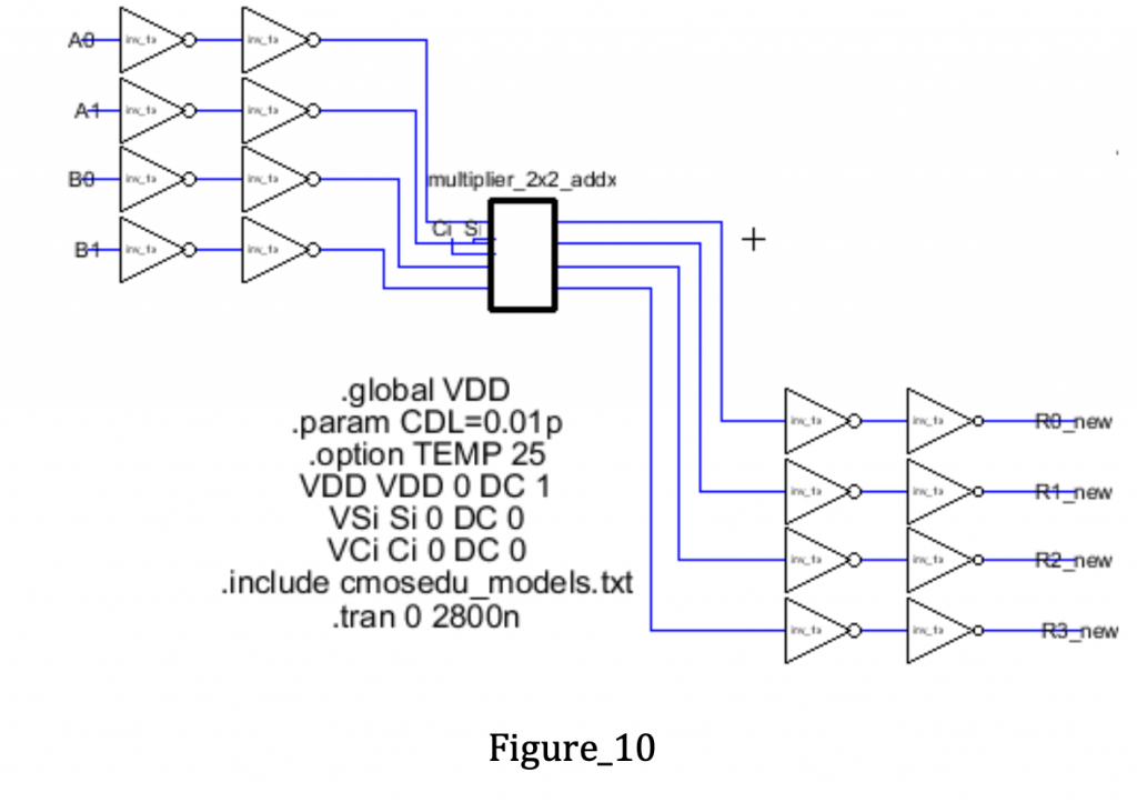
Figure_8 indicates the simulation behavior of the cell which is framed by the reference Spice waveform(https://personalpages.hs-kempten.de/~vollratj/Microelectronics/2021_Lab_Micro_Multiplier.html). There is a disturbance on the R1 at the 140ns which will be discussed in the interpretation part. Parasitic effects with driver and load inverters are taken into the account during the simulation and it will be evaluated in the delay calculation section. The same circuit was created with the VHDL feature of VLSI Electric software and the following layout (Figure_10) was built from the circuit (Figure_11) which was driver and load inverter cells attached.
The area of the 4 bits multiplier layout is measured as 605(lambda)*699.5(lambda).
——————– Cell multiplieraddx{sch} ——————–
entity addxvhdl is port( Bn,Am,Si,Ci: in Bit; S,Co: out Bit);
end addxvhdl;
architecture addxvhdl_BODY of addxvhdl is
component LUT26 port ( I0,I1 : in Bit;O: out Bit);
end component;
component LUT29 port ( I0,I1 : in Bit;O: out Bit);
end component; component LUT21 port ( I0,I1 : in Bit;O: out Bit);
end component; component LUT27 port ( I0,I1 : in Bit;O: out Bit);
end component; component MUX4 port(I0,I1,I2,I3,I4,I5 : in Bit;O: out Bit);
end component;
signal y1,y2,y3,y4 : Bit ;
begin
LUT2_1: LUT26 port map (Ci,Si,Y1);
LUT2_2: LUT29 port map (Ci,Si,Y2);
LUT2_3: LUT21 port map (Ci,Si,Y3);
LUT2_4: LUT27 port map (Ci,Si,Y4);
MUX3: MUX4 port map (Y1,Y1,Y1,Y2,Am,Bn,S);
MUX2: MUX4 port map (Y3,Y3,Y3,Y4,Am,Bn,Co);
end addxvhdl_BODY;
Comparison of Cell Performances
Two different 4 bits multipliers were designed and both have a reasonable result in simulation as pictured above. Reasonable analyses need driver and load cells to be attached to the multiplier. For this purpose, two inverters are attached to each input and output to achieve fruitful experiment results.
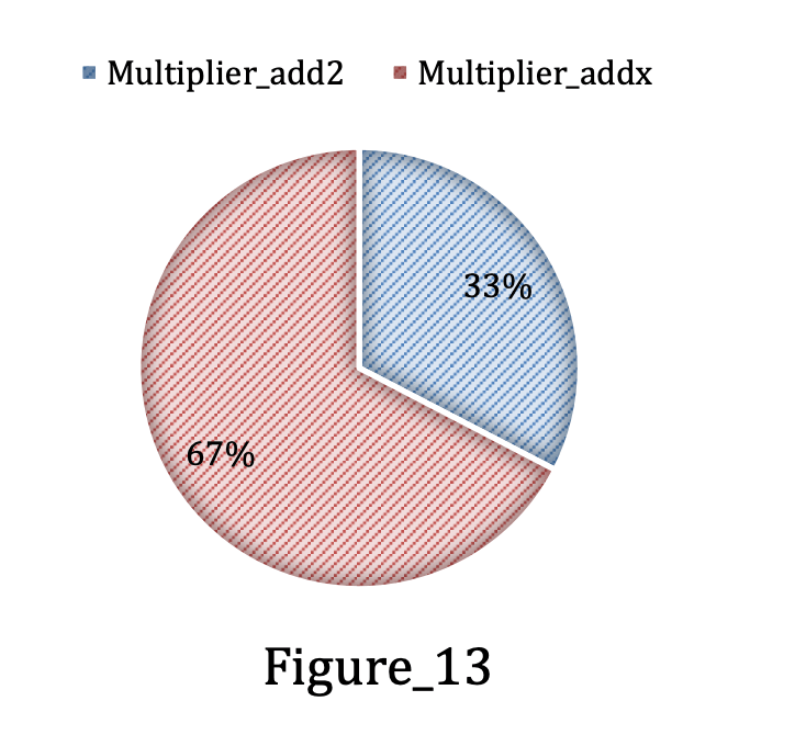
The performance comparison covers; size, delay time, and power consumption analysis. Along with the measured sizes ;
Multiplier with add2 -> 44.85 𝑭 *𝑭
Multiplier with addx ->105.8 𝑭 *𝑭
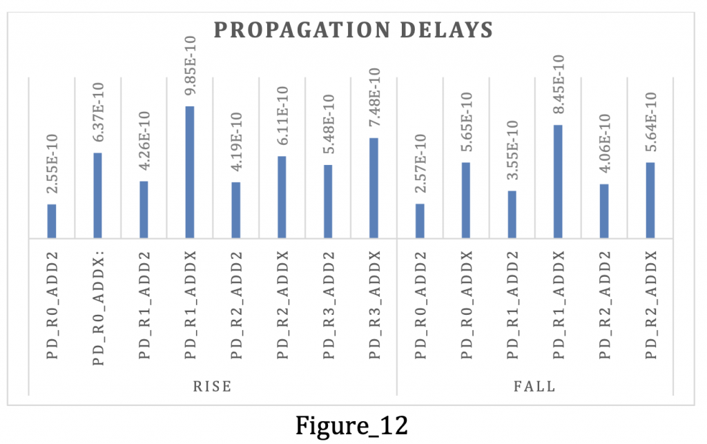
The measured delay times can be seen in the following graph with parasitic effects included analysis ;
The last comparison is power consumption has graphed on the right ;
- Add2 -> 259 mW
- Addx -> 536 mW
After the test and analysis are done, it is time to add a pad frame then finally, build an integrated circuit.
Pad Frame Addition
Pad frame is the structure that covers the die area of the chip and allows the external connections like power, ground, data -in or out. Frame generator option of VLSI Electric Software will be used for this process and relevant files are given in Microelectronics lecture notes (https://personalpages.hs- kempten.de/~vollratj/Microelectronics/2021_Lab_Micro_Multiplier.html)
In this experience, mentioned merged 4 bits multiplier circuit will be used for pad addition. The inputs and outputs equally balanced to catch square structure and relevant .txt file was edited as follows.
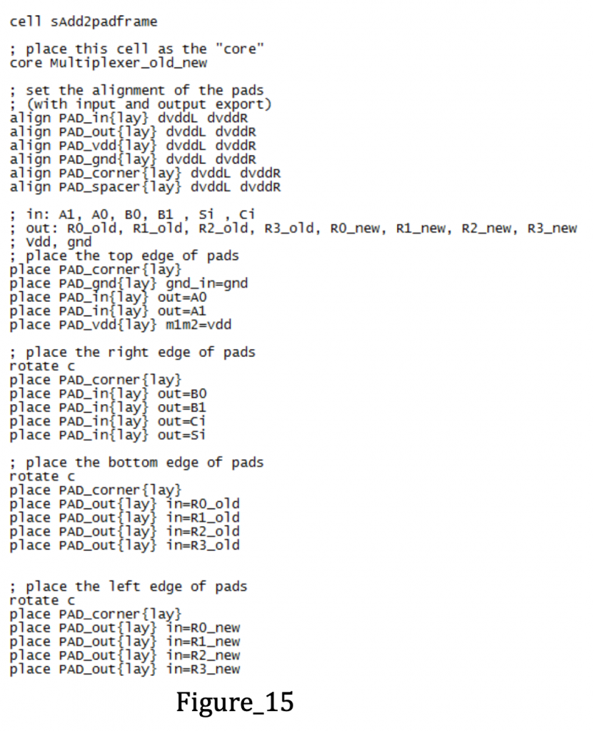
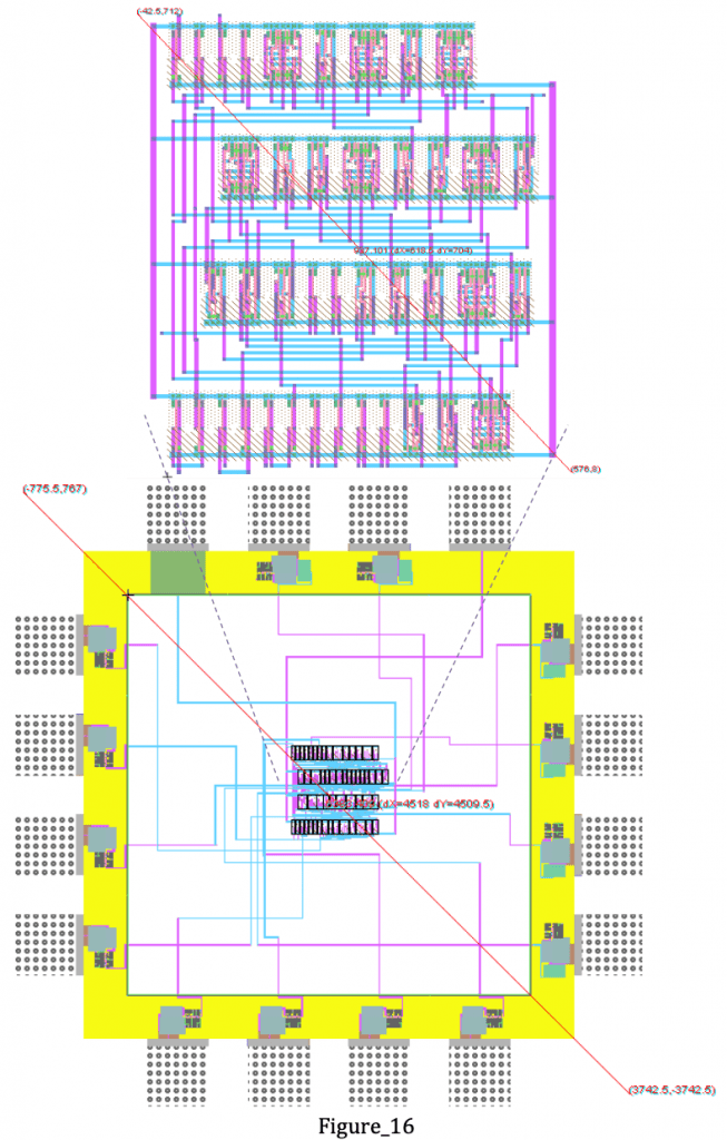
As it can be seen from the script, there is the total of 16 connections which are Vdd , GND , inputs, and outputs. Equally divided at the sides of the pad frame and required alignment elements were previously defined. The core name also changed to the same name with cell in VLSI Electric. After the successful generation of the chip structure, the internal connections were made. Merged multiplier add2 and addx layout and pad frame added version is presented on the following page.
Interpretation of Performance Results
In the final view; two types of 4 bits multipliers designed with a half adder and reusable adder block structure. The analyses in regards to size, power consumption, and delay experienced and results indicate that the multiplier with add2 has better performance than addx. As we could understand from the structure, addx unit is more way complicated than add2. Furthermore with simple brainstorming over; LUT26 has 12 MOS and LUT28 has 6 MOS which creates half adder add2. Multiplier_add2 has 2 add2 packages and 4 LUT28 which results in 84 MOS in total. Addx has two add2 and one LUT28 and LUT2E package which has 6 MOS inside. Multiplier_addx has four addx packages inside which results at the end as 216 MOS which is more than double of multiplier_add2 has. Each MOS has RC effect and it will cause delay therefore the measured results are quite reasonable with design.
Please do not hesitate to make comments or forward your questions. You can view my other articles via this link.
References
- Prof. Dr. Jörg Vollrath – Hochschule Kempten- Open Library- https://personalpages.hs- kempten.de/~vollratj/Microelectronics/2021_Lab_Micro_Multiplier.html
- Prof. Dr. Jörg Vollrath – Hochschule Kempten – Microelectronics Lecture Notes https://personalpages.hs- kempten.de/~vollratj/Microelectronics/2016_04_20_Micro_Lab03_C MOS_Inverter.html
- LTSpice – Help
- https://www.tutorialspoint.com/vlsi_design/vlsi_design_combinational_mos_logic_circuits.htm
- https://www.geeksforgeeks.org/half-adder-in-digital-logic/
- VLSI Design – Electronics
- https://tams.informatik.uni-hamburg.de/applets/hades/webdemos/05-switched/40-cmos/nand.html
- https://www.youtube.com/watch?v=EPJf4owqwdA