Thermal Performance of Discrete MOSFET Packages on PCB & Thermal Impedance Evaluation of IGBT Module - Experiment
Abstract
This scientific test covers thermal performance evaluations of both SMD – THD type of MOSFET packages and IGBT power module which attached to air-cooled heatsink. Measurement method basically for both experiments are determine to junction temperature with reference current at cooling time period of the device. MOSFET thermal performance will be evaluated under different conditions and the effects on the junction to ambient resistance will be discussed.
IGBT power module junction to case , junction to heatsink thermal impedances and thermomechanical behavior of module to be debated.
Introduction
Power MOSFETs are very popular in electronic circuits due to their affordable prices, easier manufacturing process and high input impedances. Controlling , switching and regulating are main purposes to use semiconductor devices with other benefits as well. This popularity makes MOSFET thermal performance really important matter for suppliers and buyers. Certainly , overheating or overloading of device will cause kinds of defects so thermal mapping of this devices are become inevitable for industry.
To achieve thermal network model and calculate the available thermal resistances, we need proper measurement for heat sources. For devices like a semiconductors due to thermal isolation materials and packaging it is truly challenging to determine junction temperature (Tj).
This experiment will be conducted in leading trend of measurement method which is widely used by designing engineers and approved by IEC standard (60747-9 Ed. 2.0.).
IGBT modules are also commonly used power modules. Famous by their higher switching speeds and power gains. Low conduction channel resistances make these semiconductor devices proper for higher current demand applications like UPS or frequency convertors.
This creates also thermally well performed device demand in market. Second experiment was conducted on IGBT thermal impedances and will be covered in with results.
2- Theory of Study
The basic structure of a package able to dissipate heat from the back surface consists of a lead frame (“Frame” in the Figure_1), die bonding between the chip and the lead frame, the MOSFET chip (“Chip”), and the resin package (“Mold”).
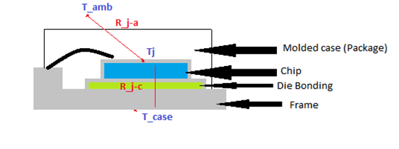
As it can be seen in Figure_1 ; red lines show thermal resistances which we can get easily from device datasheet as well.
The key power-loss contributors in a MOSFETs : conduction losses and switching losses. MOSFETs have a finite switching time, therefore, switching losses come from the dynamic voltages and currents the MOSFETs must handle during the time it takes to turn on or off.[1]
Basically , temperature differences between junction and case or junction between ambient have a correlation with total losses so calculations are going to be held with following formulas;

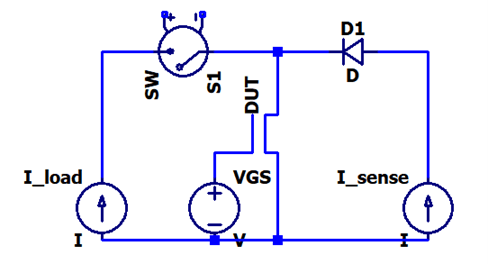
Obtained linear calibration curve of device leads spotting Tj via forward voltage measurement ( for IGBT collector to emitter voltage). Figure_2 shows the basic structural measurement circuit.
2.1- Thermal Performances of Semiconductor Devices
Three basic processes manage removal of heat from junction to the ambient air : conduction ( heat travels through the material ) , convection ( heat transfers by natural or forced air ) and radiation (propagation at electromagnetic level ). Based on the limit temperature demand , cooling process can be designed with combination of those three cooling options. Steady state and transient thermal networks can be modeled and solved.
Thermal network modeling is helpful for “Thermal Network Analyses” of semiconductor devices. The models are known Cauer and Foster which represents thermal equivalent circuit with resistors and capacitors.
In essence, the Cauer model can represent the internal physical structure of the device layers but is computationally complex to implement. In contrast, the Foster-network is easier to be complemented but cannot provide temperature changes in the internal layers of the device. In this work, the focus is placed on the junction temperature (in relation to the total thermal impedance) rather than the thermal distribution in the internal layers. [2].
In general MOSFET chips are encapsulated in plastic packaging material so this does not allow direct contact to chip. Removal of packaging material may allow us to touch chip but it is going to effect performance of cooling and probably received data can not be evaluated as real condition due to damaged isolation. Infrared cameras with the proper frame rates might be slower to measure temperature transient so implemented method is state of art currently.
IGBT modules encapsulated with ceramics and Cu (Copper) baseplate on bottom which increases cooling performance of module. But chip and body diode covered with epoxy resin. It is not that small like MOSFET but hard to measure junction temperature with the sensors inside the module also cooling performances way better than MOSFETs due to the wider surfaces for convection and baseplates for conduction.
Contactless junction temperature measurement method is become more reliable in this case.
2.2- Time Constant
Basically can be defined as a time delay. This term based on RC circuits. If the capacitor serially connected to the resistor , capacitor charges through the resistor till reaching supply voltage. The time required for the fully charge the capacitor called 5T time constant. Basically T is equals the time required to up charge %63 of steady state voltage ( V=0 , t=0).
Foster and Cauer models represents thermal networks with RC structure so heating up can be simulated as a charging process of capacitor. Due to this analogy charging and discharging time constants will be considered.
2.3- Experiment Method
The method simply works with body -diode forward voltage (V_f) response to the temperature changes.
When operating with a small measurement current which will be mentioned as I_sense , bipolar semiconductors show a linear dependency between the forward voltage drop and the chip temperature. A calibration curve V_CE=f(Tj) or V_f=f(Tj) is generated using this effect by passive heating and measuring the forward voltage at the measurement current and different temperatures.
Then the switch MOSFET or IGBT is operated at a constant load current to heat it until thermal equilibrium is reached. The power dissipation is calculated by P_loss=V_CE*I_load.
After switching off the load current the small measurement current is applied to the switch. T_j can be derived from the measured voltage drop by the calibration curve a few 50 μs after turning off. The short brake is necessary to allow semiconductor charge carrier effects to decline. The result is an area related average junction temperature of that switch.[5]
Important part to remember; measurement current (I_sense) should be selected small enough to avoid heating up device.
For MOSFET experiment calibration line linear equation which will lead T_j measurement is given below;

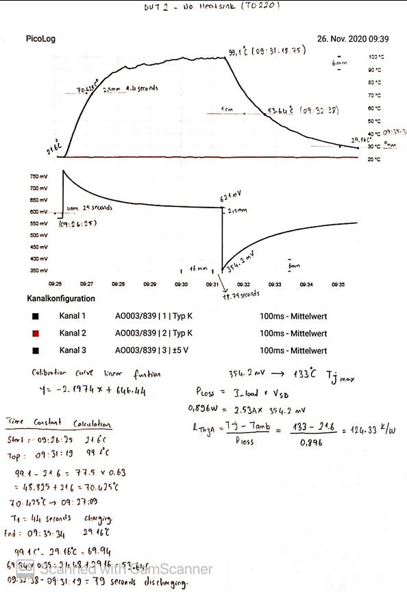
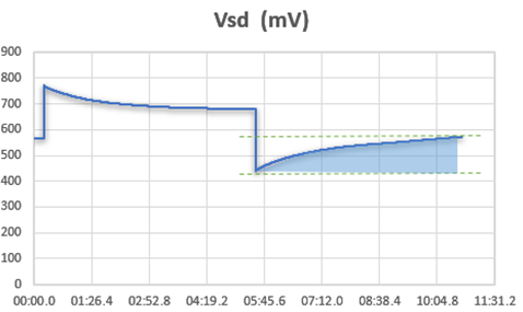
Figure_3 shows cooling-down area of TO220 package from second experiment and V_SD rise in time function.
2.4– I_load Calculation For Both Experiments
Before starting experiment I_load current should be determined to heat up device.

To keep T_j less than 125 C related P_loss can be calculated with Eq_2;
For THD R_thjA = 62 K/W and for SMD R_thjA = 75 K/W can be obtained from datasheets [3] and calculated power losses stated below;

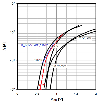
R_bd can be determined the inclination of assumed 125 C curve at Figure_4 as 10 miliohm.

Finally , from Eq_3 , I_load current can be calculated as 2.53 A for THD and 2.09 A for SM device.
3- Execution of MOSFET Experiment
In this experiment TO262 ,TO220 , TO252 Infineon [3] type SMD and THD MOSFET will be investigated with following conditions;
- Board Horizontal without fan convection (TO262)
- Board Horizontal with 10V supplied fan convection (TO262)
- Board Horizontal without heatsink (TO220)
- Board Horizontal with heatsink (TO220)
- Board Vertical without fan (TO252 with 105 µm Cu PCB)
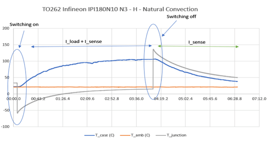
Temperature sensor is taped around case and V_SD has been monitored via +5V TC-08 Data Logger input card. 6mA , I_sense connected source-drain terminal from LT3092 programmable current source. TH Device T0262 has connected and switched on with I_load = 2.53A and I_sense=6mA then rise of T_case has been followed on PicoLog software.
When DUT reached to steady state , I_load switched off and the change of V_SD monitored till T_amb almost equals to T_case.
For second experiment on TO262 conducted with 10V supplied fan (SANYO 9G0612P4S001). THD switched on with 2.53A I_load and steady state achieved , switched off then results have recorded. Thermal performance of device under forced convection has examined.
TO220 has tested with natural convection as well. 2.53A I_load has applied and voltage between source – drain terminals (V_SD) has recorded with datalogger. The difference between TO220 and TO262 packages ; TO220 package has a hole extension to mount it causes longer base frame. It can be simply seen Figure_6.
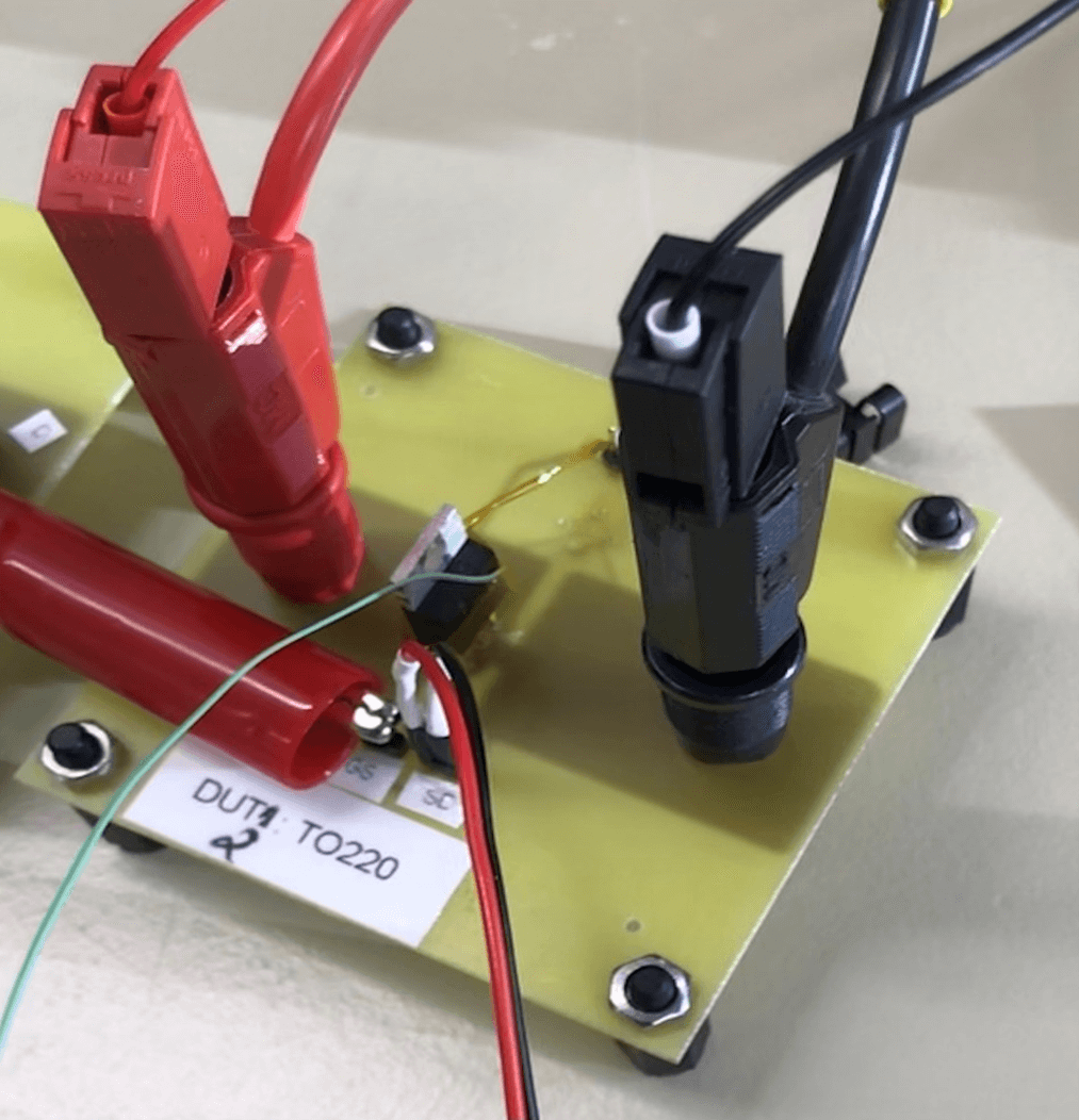
This experiment is repeated with heatsink mounted TO220 package. Heating and cooling period has investigated and recorded.
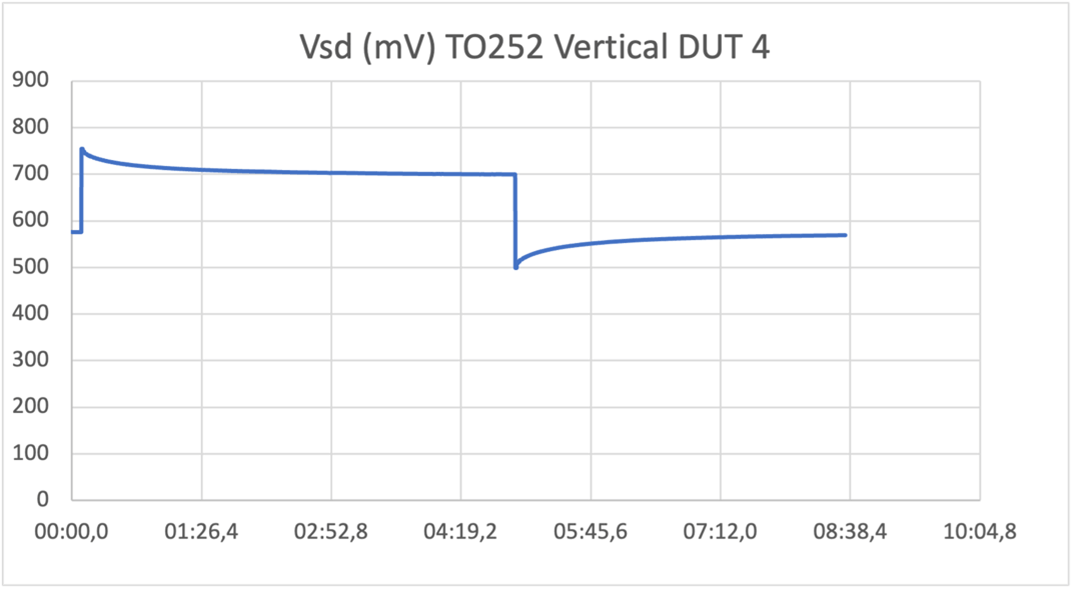
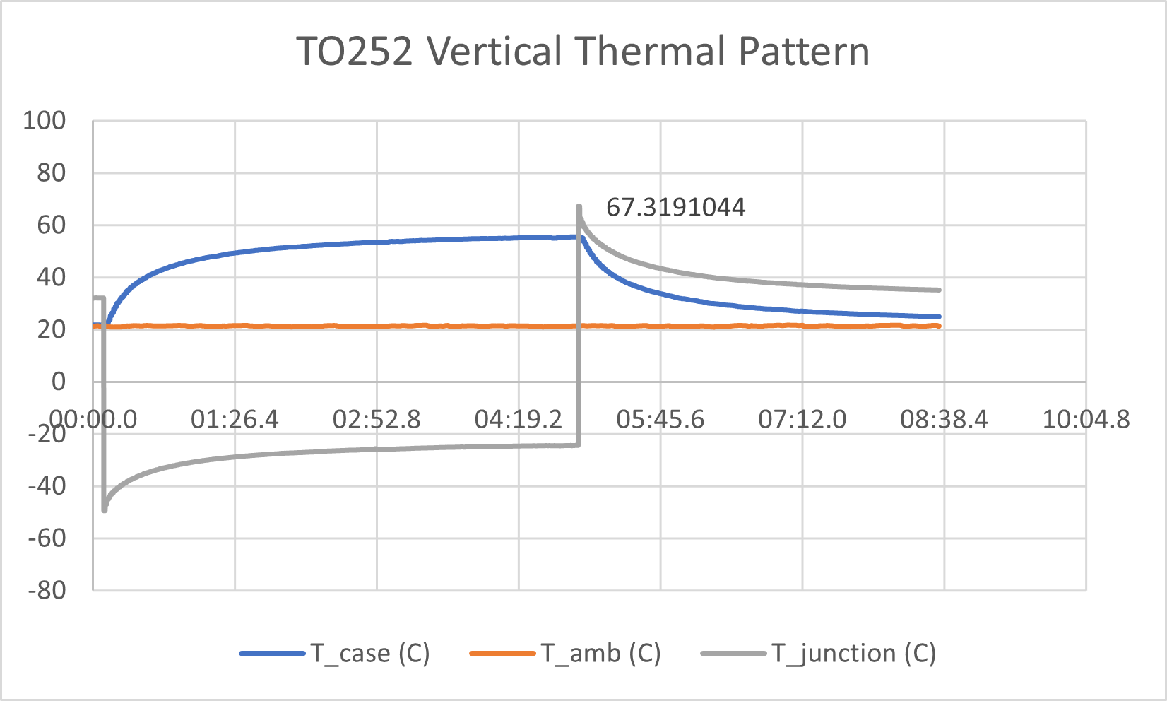
All experiments up to now was conducted at horizontal form. Next experiment was done on TO252 with 105µm Cu layer which placed vertically. Due to the higher R_thjA (75 K/W) , I_load current for SMD device is re-calculated and applied as 2.09A. Thermal performance and recorded V_SD visualized at Figure_7

Three different MOSFET packages and thermal performances have tested under different conditions. Actual V_SD , T_case and T_amb values are recorded by datalogger.
4– Execution of IGBT Experiment
Purpose of this experiment measuring thermal impedance of IGBT module Infineon FF50R12TR4 [4] which is attached air-cooled heatsink. Sensor is located under the chip in thermal interface layer for case temperature measurement. Gate terminal has switched with 10V bias so loading device will cause heat losses. Voltage changes between collector-emitter terminals (V_CE) were monitored with oscilloscope (Keysight DSOX2024A). Switching the IGBT module was done with two n-channel MOSFET and triggered by signal generator due to make switching more quicker. 39.4mA , I_sense current between emitter and collector terminals provided by LT3092 programmable current source.
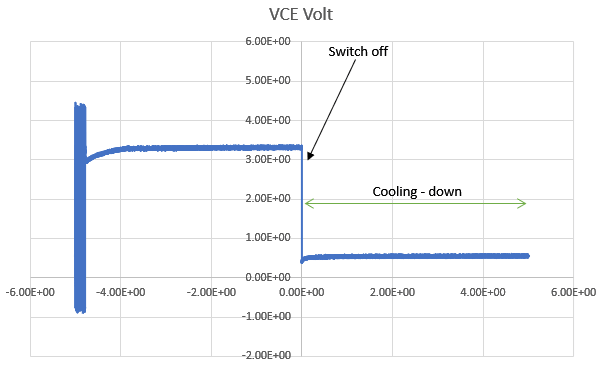
IGBT module was switched-on and off couple of times with 40A I_load in proper scale arrangement (50µs,100µs,1ms,10ms,100ms) to investigate cooling down process better. V_CE values on oscilloscope screen can be seen similar as Figure_8 below.
Experiment was repeated to measure heatsink temperature pattern and thermal resistance with same voltage, current values but different test settings.
5- Results
This section covers experimental results of each test for regarded power semiconductor devices. Microsoft Excel and Picolog softwares are used to process and visualize data then interpretations will be mentioned in discussion part.
5.1– TO262 on PC Board Horizontal Without Fan Convection
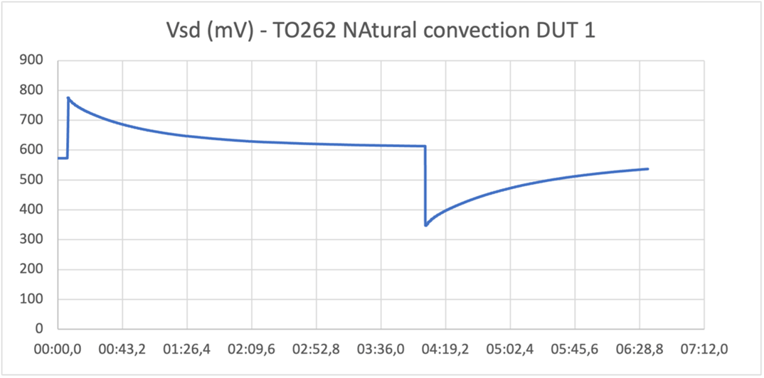
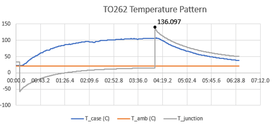
Device has switched on with 2.53A I_load and I_sense 6mA then the temperature pattern of TO262 package can be seen in Figure_9.
As device reach the steady state value , the junction temperature marked 136.097 C and maximum case temperature has recorded as 106.694 C .
Time constant (T) due to capacitor effect while heating up the device is calculated as 58 seconds for TO262 package.
R_thjA = 130.747 K/W (max) can be easily derived from Eq_2.
5.2- TO262 on PC Board Horizontal with 10V Supplied Fan Convection
Fan placed next to PCB to provide forced-air convection to device and energized with 10V DC. TO262 package switched on with 2.53A I_load and I_sense 6mA again then temperature rise monitored at Picolog Software.
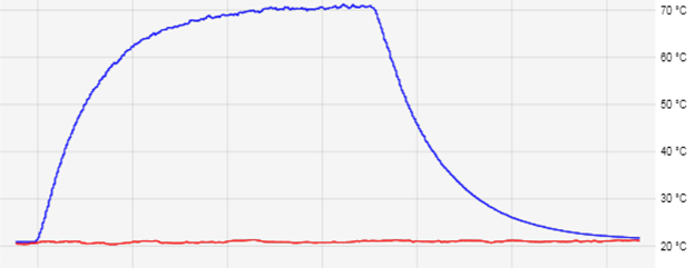
T_j which is quite closely plotted at 99.15 C. Maximum case temperature of device touched 71 C can be seen in Figure_10.
R_thjA = 72.36 K/W (max)
Time constant (T) for TO262 charging curve with forced-air convection effect is 36 seconds.
5.3- TO220 on PC Board Horizontal Without Heatsink
In this experiment power module has changed with hole mounting type which called TO220. Cables are connected and experiment started with 2.53 A I_load current and I_sense 6mA.
During the experiment steady state has reached at 99.1 C , T_case. Maximum T_j has recorded 133.41 C. Time Constant (T) is calculated as 44 seconds.
R_thjA = 124.33 K/W (max)
Note: During previous two experiment due to software language ; sampling time settings of .cvs raw data save option on Picolog was not set properly. Regarded analyses have done with Picolog graph (e.g Figure_10) manually and precisely. Related documents shared in appendix section.
5.4- TO220 on PC Board Horizontal with Heatsink
This experiment conducted to explore heatsink effect on semiconductor devices.
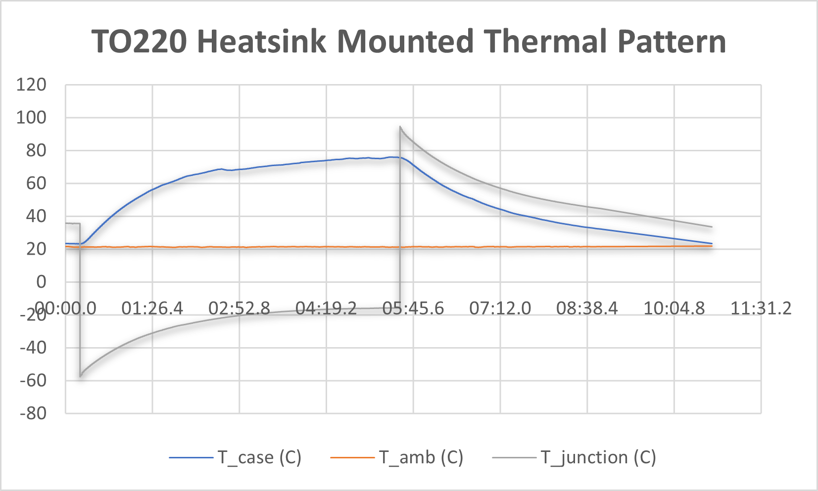
Heatsink mounted previous TO220 package has energized with I_load 2.53 A and I_sense 6mA. Heating up process was monitored.
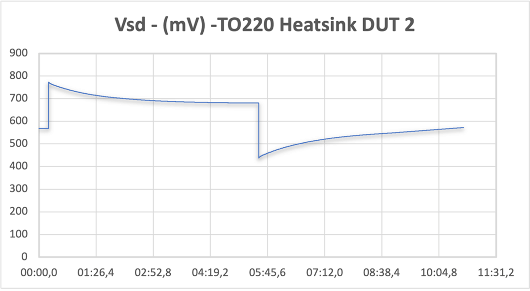
T_case reached equilibrium at 76.065 C and T_j max is calculated as 94.68 C. First Time Constant (T) is 74 seconds.
R_thjA = 66.18 K/W (max)
5.5- TO252 on PC Board Vertical (with 105 µm Cu PCB)
This experiment was conducted with SMD type device TO252 package.
Device vertically positioned then switched with 2.09 A I_load and I_sense 6mA current. After reaching steady state I_load current switched off and cooling – down process has recorded. Maximum T_j calculated as 67.31 C and T_case has reached 55.61 C
Charging Time Constant for SMD TO252 calculated as 36 seconds.
R_thjA = 44.06 K/W (max)
5.6- Heatsink Attached FF50R12TR4 IGBT Module
Infineon FF50R12TR4 [4] has tested with low – side switch and high – side switch settings. Due to resolution difference between Picolog and oscilloscope, linear interpolation has been done for time interval less than 100 miliseconds.
I_sense= 39.4mA , I_load = 40A and V_CE = 3,29 V was recorded before turn-off the device and power loss for this operation calculated as 132.09 W.
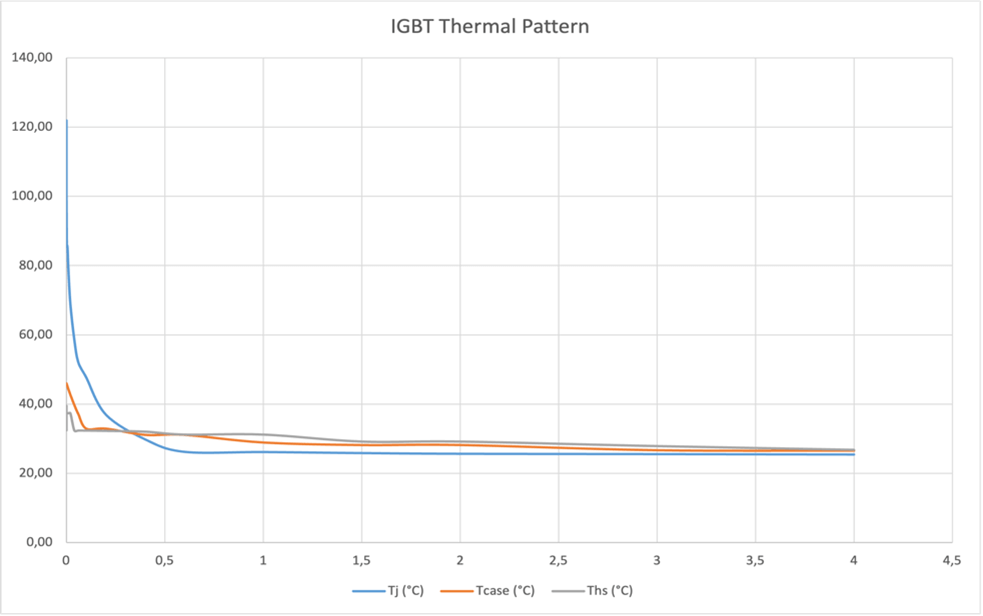
Max T_j= 121.99 C and Max T_case= 46.02 C can be seen in graph. (Figure_13)
R_thjc Max =0.58 K/W
R_thjhs Typ = 0.25 K/W
Steady state thermal resistances has calculated as stated above and measured thermal impedances in logarithmic time scale plotted for discussion in Figure_15.
6- Discussion
Results are stated below once more to Figure_14 to visualize to comparison.
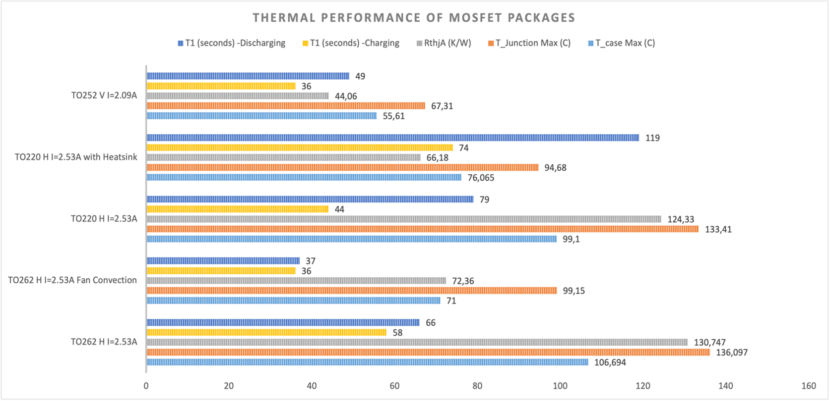
Package temperatures are all stay inside design temperature range. Result of typical thermal performance improvements may give significant differences. Listed 5 experiment results can be compared and interpreted;
In first-two experiment with TO262 , fan convection makes almost 37 C drop both junction and case temperatures. Effect of reduced temperature difference between junction and ambient can be seen in difference of thermal resistance parameters. Based on the instructions ; junction temperature should have stayed less than 125 C but it was not for some test. Accordingly load current has selected slightly higher. It might cause that calculated thermal resistances are higher than datasheet value due to higher junction temperature and lower V_sd. Forced convection caused quicker reach to steady state so time constant is less than natural convection as well but individual discharging and charging time constants are quite similar. Operate TO262 with fan convection apparently increase reliability and lifetime of the product.
Second-two experiment demonstrates heatsink effects on TO220 cooling performance. Before discussing about heatsink effect , comparison of TO262 and TO220 packages show us due to bit longer base lead of TO220 , cooling performance on natural convection is not significantly but better than TO262 package and junction temperature stayed under 125 C.
It also causes drop the junction to ambient resistance. Initially can say ; longer base lead or mounting lead improves thermal performance of devices.
As expected heatsink would improve the thermal performances and in this experiment it make 39 degree difference in maximum junction temperature which is surprisingly high. If we compare the size of heatsink with fan, heatsink effect completely can not be denied. Due to reduction on power loss and maximum junction temperature , junction to ambient resistance dropped also almost half compared to the natural convection. The time passed up to reach thermal steady state for heat sink experiment is more than 5 minutes which is generally around 4 minutes for others. This caused longer time constant also TO220 has longer time constant than TO262 with natural convection conditions. It literally means increased cooling surface causes longer charging time period. However , heatsink can be effective solution to improve thermal performance of semiconductor devices , especially when it comes to save from space.
Vertically placed TO252 package is surface mounted device. In this case surface improvement plays quite important role cause the conduction will be the key part of cooling process. Therefore this PCB board is supported with 105 µm Cu to upgrade thermal performance. Calculated thermal resistance in experiment is less than datasheet due to vertical forced convection effect. Also it can be derived from comparison that vertical positioning effects convection coefficient more than horizontal positioning. It might be a consequence by hitting effect in vertical positioning leads more quicker flow change between warm air and cool air. At the same time distance of forced air source and spreading of air matters as well. Charging time constant is low as well to compare with others and almost similar with horizontal forced convection experiment of TO262.
IGBT module thermal pattern (Figure_13) demonstrates forced convection and heatsink effect is remarkably effective of cooling performance. It is inevitable that ceramic packaging and bigger surface are significantly improve the cooling performance however with the air-cooled heat sink , junction temperature has dropped ambient temperature after a second.
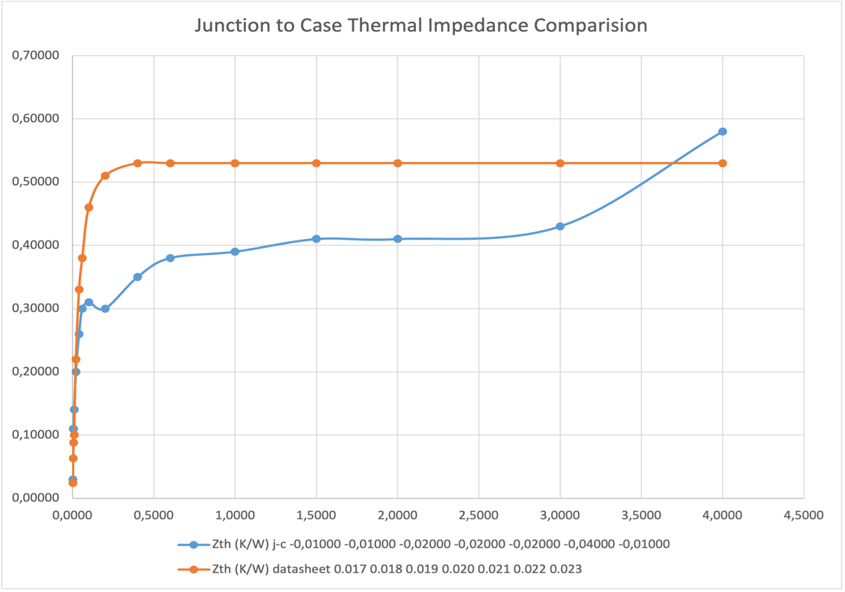
Measured thermal impedances are reasonably close to thermal impedance curve in datasheet. At the end of cooling process junction temperature and case temperature became quite closer therefore almost t=0 , Z_th max gives similar results. Steady state thermal resistance is stated R_thjc 0,84 K/W max and R_thjhs 0,12 K/W tpy. in datasheet.
Deviations accumulated mostly around 50-400 μs scale so the reason is probably T_case approximation. Due to this reason also R_thjc can not be spotted closely. Acquiring more precise data if its possible with 50 μs scale with Picolog or other software could help better approach.
7- Conclusion and Outlook
Theoretically studied methods and improvements like forced or natural convection, conduction and heatsink effects to cooling performance of semiconductor devices have experimented and discussed. The method IEC standard (60747-9 Ed. 2.0.) is quite functional to measure junction temperature of the semiconductor devices and make related analyses with it. Thermal mapping of devices are quite easy but at the same time it needs precise measurement process. The derived results are in parallel with datasheets however there are some deviations due to scale approximation. It is also proven that there are quite many options and technologies to improve thermal performance of semiconductor devices but also there is cost and performance balance should be kept. That is what we engineers do ; to find best solution with all benefits.
References
[1]- G. Lakkas – Product Marketing Manager, Power Management “MOSFET power losses and how they affect power-supply efficiency”
[2] – H. Chen, B. Ji, Member, IEEE, V. Pickert, Member, IEEE, W. Cao, Senior Member, IEEE “Real-Time Temperature Estimation for Power MOSFETs Considering Thermal Aging Effects “ , 2013.
[3] -TO262-TO220-TO252 Datasheets ;
• https://www.infineon.com/dgdl/Infineon-IPP180N10N3_G-DS-v02_02-en.pdf?fileId=db3a30432239cccd01226066faa07f9d
• https://www.infineon.com/dgdl/Infineon-IPD180N10N3_G-DS-v02_03-en.pdf?fileId=db3a30432239cccd01226070a4bb7fb9
[4] FF50R12RT4 IGBT Module Datasheet ;
• https://www.infineon.com/dgdl/Infineon-FF50R12RT4-DS-v02_00-en_de.pdf?fileId=db3a304327b89750012805fb1a356147
Appendix
